-
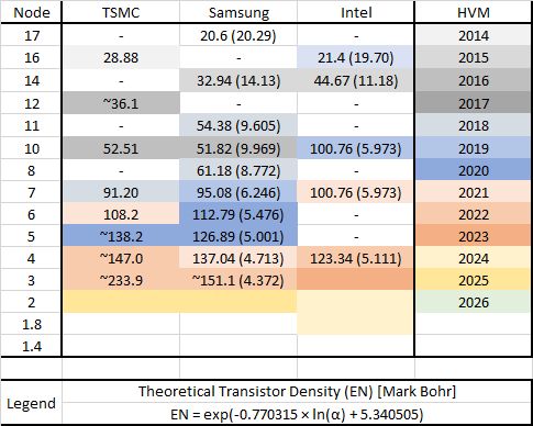
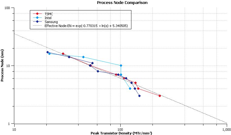
Process Node Table/Graph Update: The major differences are regarding Intel 4, TSMC N6/N5, Samsung 4LPE and derivatives therein. There's a lot of other changes, but you'll have to compare them manually for that.Permalink On twitter.com
 ♻️ 17 Retweets
❤️ 90 Favorites
Mood 0
♻️ 17 Retweets
❤️ 90 Favorites
Mood 0
-
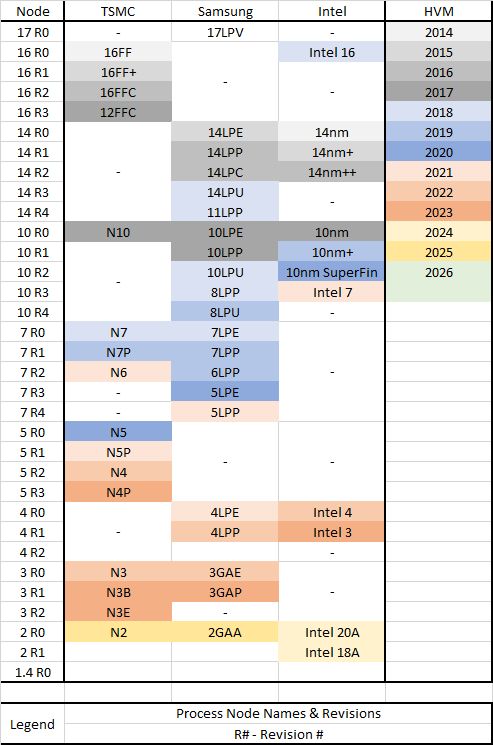
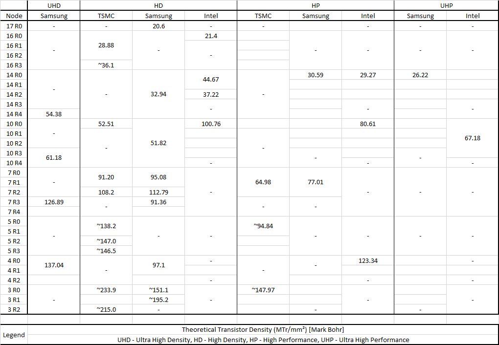
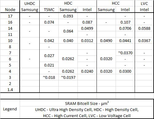
Here's tables of each node's revisions, library densities, where possible, and SRAM bitcell sizes. The node names are a complete mess, but it's the only way I could account for 14nm++ and N3E decreasing in density, as well as 12FFC, N6, 6LPP, 3GAP, etc. increasing in density.Permalink On twitter.com
♻️ 2 Retweets
❤️ 22 Favorites
Mood -2 🙁
-
Fun Facts: For every 2x shrink in node name, there's ~1.7x shrink in density. TSMC states +6% density on N4P, but also -6% area on N4, meaning a naive calculation says N4 is denser. Samsung added UHD SRAM with 5LPP and continued it on 4LPE, but has yet to reveal its size.Permalink On twitter.com
♻️ 1 Retweets
❤️ 21 Favorites
Mood +2 🙂
-
Bonuses for anyone that follows me: Samsung 3GAP: ~195.2 TSMC N3E: ~215.9 There's also a mistake in N3, it should be ~234.9, not ~233.9.Permalink On twitter.com
❤️ 9 Favorites
Mood -2 🙁
-
Small Update, I had completely missed out on this, but TSMC disclosed the HP (HCC) SRAM bitcell size on N5, its 0.025 μm², making it the third densest bitcell disclosed to date, after only N5 HD and I4 HD.On twitter.com
♻️ 1 Retweets
❤️ 5 Favorites
Mood -2 🙁